Application Closes In:
Days
Hours
Minutes
Sec
Build the Brains of Tomorrow's Tech
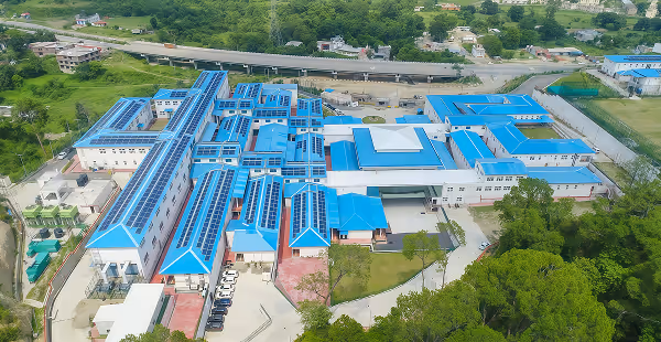
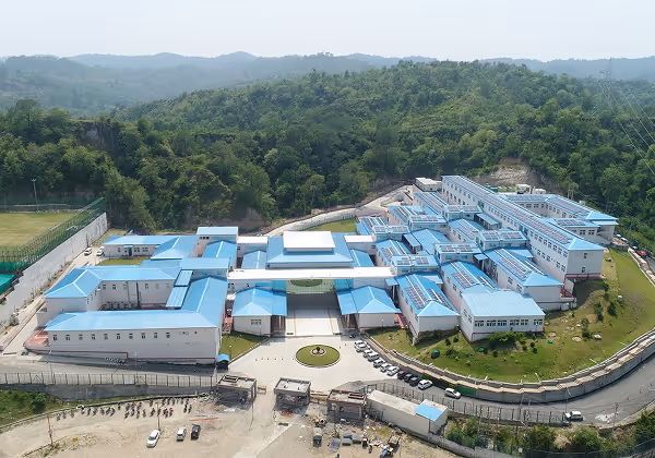
The Indian Institute of Technology Jammu is a premier Institute of National Importance committed to technological education, research, and innovation. In 2018, IIT Jammu relocated its primary operations to a sprawling 400-acre campus in Jagti village, situated along National Highway-44, just 17 km from Jammu Airport and 19 km from Jammu Tawi Railway Station.
Phase 1A of the main campus, covering 25 acres, is fully operational, while Phase 1B and 1C are under rapid construction. The Paloura campus hosts the Central Instrumentation Facility (CIF / SAPTARSHI Labs), a cutting-edge research facility equipped with advanced instruments supporting researchers in basic sciences and engineering.
IIT Jammu's VLSI Design program exemplifies its vision to create humanistic technology driven by design and innovation. Guided by the motto "Learn, Engage, Invent, Create Impact," the institute fosters a culture of mutual respect, creativity, collaboration, and innovative problem-solving. With infrastructure designed to sustain cutting-edge research and a goal to create regional, national, and global impact, IIT Jammu is not just an institution, it is a legacy in the making.

Dr. Satyadev Ahlawat is currently serving as an Assistant Professor in the Department of Electrical Engineering at IIT Jammu. He received his Ph.D. in Electrical Engineering from IIT Bombay, where he also worked as a Research Scientist in the CADS Laboratory. He has held positions as a Teaching Assistant at IIT Bombay, Lecturer at Kurukshetra University, and Research Assistant at the Indian Institute of Science, Bangalore.
His primary research interests include VLSI testing and Design-for-Test (DfT) architectures, trusted system design, hardware security, and high-performance processor design. He has taught courses in VLSI design and test, cryptography and hardware security, semiconductor device physics and technology, and computer architecture, and has contributed to several collaborative research projects. His academic credentials include an M.Tech in Microelectronics from Panjab University and an M.Sc. in Electronics from Kurukshetra University.
Under his guidance, the M.Tech in VLSI Design at IIT Jammu equips learners with both the theoretical foundations and applied engineering skills needed to design, verify, and deploy next-generation semiconductor systems.
Earn a prestigious M.Tech (Executive) degree from IIT Jammu, a Premier Institute of National Importance, representing academic excellence and deep-tech specialization in VLSI Design and Intelligent Systems, along with IIT Jammu Executive Alumni Status.
in Just 24 Months
Year 1: Semester 1
Year 1: Semester 2
Year 2 : Semester 3
Year 2 : Semester 4
Elective Course Options
Low Power Circuits and Systems, Physics of Transistor, Reliability of VLSI Circuits, Test and Verification of SoCs, Embedded System Design, Computer Architecture, Semiconductor Devices for High Frequency, Design for Manufacturability of VLSI Circuits, Cyber Physical Systems, Compact Modeling of Semiconductor Devices, Mixed Signal Circuit Design, Digital VLSI Architecture Design, MOS Device Modeling, Intelligent Systems with VLSI*, Integrated Circuit Design with Networking Protocols*, VLSI Design in IoT System Design*, VLSI for Automotive Electronics*
*Approval under process. Electives are subject to faculty availability and discretion of the Program Coordinator.


Through the Futurense AI Clinic, you'll gain hands-on exposure to real enterprise-grade AI and data engineering projects.
Solve real industry-grade VLSI challenges by designing and verifying digital, analog, and mixed-signal integrated circuits across application domains like consumer electronics, automotive, and telecommunications.
Gain hands-on experience with full-cycle EDA flows using Cadence, Synopsys, and Mentor Graphics, the same tools used by leading semiconductor firms globally.
Guided by IIT Jammu faculty and Futurense Leadership Council industry mentors at every stage, from problem definition and design specification to simulation, verification, and final delivery.
Learn how to take a chip design from concept to prototype, covering CMOS circuit design, ASIC flows, simulation, layout, and readiness for real-world deployment.


BE / B.Tech / M.Sc. in ECE, EE, ETC, CSE, ME, Physics, or a related field.
Minimum 2 years of full-time industry experience is compulsory.
Minimum 60% or 6.0 CGPA in Under-Graduation or Post-Graduation. (55% or 5.5 CGPA for candidates with over 10 years of work experience.)
Pre-Screening Test (Technical + Aptitude Based)
What You’ll Be Tested On
Duration: 120 minutes
Hardware engineers, PCB designers, and embedded systems developers looking to transition into core VLSI design, ASIC development, or chip architecture roles.
Professionals working in semiconductor firms, EDA tool companies, or R&D labs seeking to deepen their VLSI expertise and take on advanced design roles.
Working professionals in electronics, automotive, or defense sectors who want to specialise in VLSI design and move into high-value IC/chip design positions.
Early-career engineers and STEM graduates aiming for an IIT-credentialed VLSI specialization to accelerate career growth and unlock high-demand roles in India's booming semiconductor industry.

Craft a recruiter-ready identity with optimized resumes, LinkedIn profiles, and a strong career narrative.

Develop job-ready skills with role-focused training, capability tests, AI tools workshops, and continuous upskilling to match real hiring expectations.

Access curated, pre-vetted roles before they hit public portals, with priority visibility for Futurense learners.

Get insider interview guidance with structured playbooks: FAQs, sample answers, frameworks, recruiter insights, and round-wise preparation.

Experience real interview simulations with personalized feedback from mentors, industry leaders, and FLC members.

Unlock referral advantages, insider recommendations, alumni-driven opportunities, and FLC mentorship that accelerates your career entry.

Get guidance on positioning, benchmarking, negotiation strategy, and communication to secure the compensation you deserve.
They are working at companies which are a dream for most


| Component | Amount (₹) |
|---|---|
| Program Fee (Year 1) | ₹3,37,000 |
| Program Fee (Year 2) | ₹1,81,000 |
| Registration Fee (Non-refundable)** | ₹10,000 (Included in Year 1 fee) |
| Total Program Fee* | ₹4,49,000 |

Admissions close once the required number of students is enrolled for the upcoming cohort. Apply early to secure your seat.
How it Works
Submit your application online and complete the pre-screening test. Pay the registration fee to confirm your intent.
Clear the pre-screening test and receive your official offer letter from IIT Jodhpur. Complete your full program fee payment to secure your seat.
Strengthen your foundations through the Futurense Bridge Course and begin your live online weekend sessions with IIT Jammu faculty, along with mandatory campus immersion in Year 1.
Kick things off with a 2-Week Bridge Course that gets you course-ready.

Worth ₹29,000
A collective of CXOs, AI leaders, and digital transformation heads from global and Fortune 500 companies shaping the AI-native workforce.


Become the VLSI engineer who designs, verifies, and deploys the semiconductor systems that industries now depend on — from smartphones and EVs to AI accelerators and 5G infrastructure.
We know you might have some questions before getting started in our platform
The program is called the Executive Post Graduate Certification in AI-Enabled VLSI Design and it is offered by the Indian Institute of Technology Kharagpur (IIT Kharagpur).
The program duration is approximately 8 months, with the next cohort tentatively scheduled to begin in June 2026.
Criteria:
1. B.Tech/M.Tech or B.E/M.E (final-year students or graduates).
2. Acceptable disciplines include Electronics, ECE, Electrical Engineering, VLSI, Instrumentation, Computer Science, and IT.
3. M.Sc. in Electronics, Physics, or Semiconductor Technology, or MCA is also accepted.
4. Minimum 50% aggregate marks or equivalent CGPA from a recognized university.
Ideal Candidates:1. 4th-year engineering students interested in VLSI design.
2. Fresh graduates looking to start a career in semiconductor and chip design.
3. Working professionals seeking to transition into VLSI roles.
4. Candidates from other engineering backgrounds with exposure to digital electronics, HDL, embedded systems, or semiconductor fundamentals.
Applicants can apply online by completing the application form and submitting their personal, educational, and professional details along with the required documents.
The application process has already begun, and candidates can apply while seats are still available.
Yes. The selection process involves submitting an application, a profile review by the technical committee, and a pre-screening test to assess subject knowledge before receiving the final offer letter.
Applicants must submit documents such as Aadhar Card, date of birth proof, resume, graduation marksheets and degree certificates, 12th marksheet, and work experience documents if applicable.
Yes. A pre-screening test evaluates candidates’ understanding of digital electronics, analog electronics, logical reasoning, and Verilog fundamentals.
Basic knowledge of Verilog coding is recommended to perform well in the pre-screening test and to start the program smoothly.
The program is delivered through 100% live online classes conducted by IIT Kharagpur faculty and industry experts.
Yes. Participants who choose to attend the optional campus immersion will need to pay approximately ₹10,000 closer to the immersion dates.
Yes. Accommodation booking can be facilitated for outstation candidates during the campus immersion, subject to availability.
The program integrates industry-grade Cadence tools, the Vivado FPGA workflow, and a complete RTL-to-GDSII design flow enhanced with AI-driven PPA optimization and low-power design techniques.
The program is led by Prof. Mrigank Sharad, whose expertise in nanoelectronics, VLSI design, and digital and mixed-signal systems contributes to developing energy-efficient AI hardware and modern semiconductor technologies.
Established in 1951 as India’s first IIT, IIT Kharagpur has a strong legacy in engineering education and advanced semiconductor research, combining academic rigor with industry-relevant curriculum design.
Industry practices and modern semiconductor workflows are integrated into the curriculum, ensuring that learners gain exposure to real-world design methodologies and AI-enabled chip design practices.
The curriculum covers digital design foundations, Verilog-based RTL development, FPGA workflows, ASIC implementation, low-power design, and the complete RTL-to-GDSII design lifecycle including timing analysis and physical design.
Participants gain hands-on experience with tools such as Vivado IDE and Cadence tools including Xcelium, Genus, Innovus, Tempus, and Voltus. The program also includes Verilog programming and basic TCL scripting.
The program integrates AI-driven workflows including machine-learning-based design space exploration, predictive static timing analysis, and AI-guided optimization of power, performance, and area metrics.
The program offers full-stack exposure from RTL design to GDSII implementation using commercial-grade semiconductor toolchains and AI-enabled automation workflows.
Through modular learning and customizable capstone projects, participants can focus on areas aligned with their interests within semiconductor design.
Participants work on projects such as hardware-accelerated audio signal processing with neural network classifiers, Tiny-YOLO based object detection accelerators, and optical flow estimation accelerators for automated vehicles.
Graduates can pursue roles such as RTL Design Engineer, FPGA Design Engineer, ASIC Implementation Engineer, Physical Design Engineer, Low-Power Design Specialist, and AI-EDA Integration Specialist.
AI-integrated EDA skills are highly valued in the semiconductor industry and open access to specialized roles with higher compensation potential.
The program equips learners with both traditional VLSI methodologies and emerging AI-driven automation skills, preparing them for the evolving semiconductor ecosystem.
Upon successful completion, participants receive the Executive Post Graduate Certification in AI-Enabled VLSI Design from IIT Kharagpur.
The program fee is ₹1,25,000 plus 18% GST. Financing options are available through partner financial institutions.
A non-refundable application deposit of ₹5,000 must be paid during application submission and is adjusted in the final fee. The remaining fee must be paid within five days of receiving the offer letter.
Yes. Participants can self-fund the program either fully or partially through personal or family resources.
Yes. Futurense partners with financial institutions to help eligible participants access loan options.
Interest rates vary depending on the financial partner and repayment plan and are generally competitive in the current lending market.
Applicants should keep their:
1. PAN card.
2. Aadhaar card.
3. Bank statements for the last three months (required for financing or loan processing).