.avif)


The VLSI full form is Very Large Scale Integration. You can consider it as the process of integrating thousands or even millions of electronic components onto a single silicon chip. These components can be transistors, resistors, and capacitors.
VLSI technology forms the foundation of modern electronics. Every digital device we use is made possible only through VLSI design. From our smartphones and smartwatches to high-performance processors, all utilize this technology.
This article will clearly explain the VLSI design flow, including the physical design flow in VLSI and the VLSI design flow diagram. So, let’s understand how the complete process actually takes place!
What is VLSI Design?
VLSI design is simply the art and science of creating integrated circuits. These circuits have specific functionality, performance, and power requirements. The process involves several stages that go from system-level planning to transistor-level implementation.
To become sure of accuracy and manufacturability, the design is divided into two main parts:
- Front-End Design: It focuses on functionality and logic.
- Back-End Design: This part of the design focuses on the physical layout and fabrication of the system.
Together, these two form the VLSI Design Flow.
VLSI Design Flow Overview
The VLSI design flow defines the systematic sequence of steps that we follow to convert an idea into a working silicon chip. Each new stage depends upon the previous one. To ensure that the design is functionally correct and physically realizable, each stage is equally important.
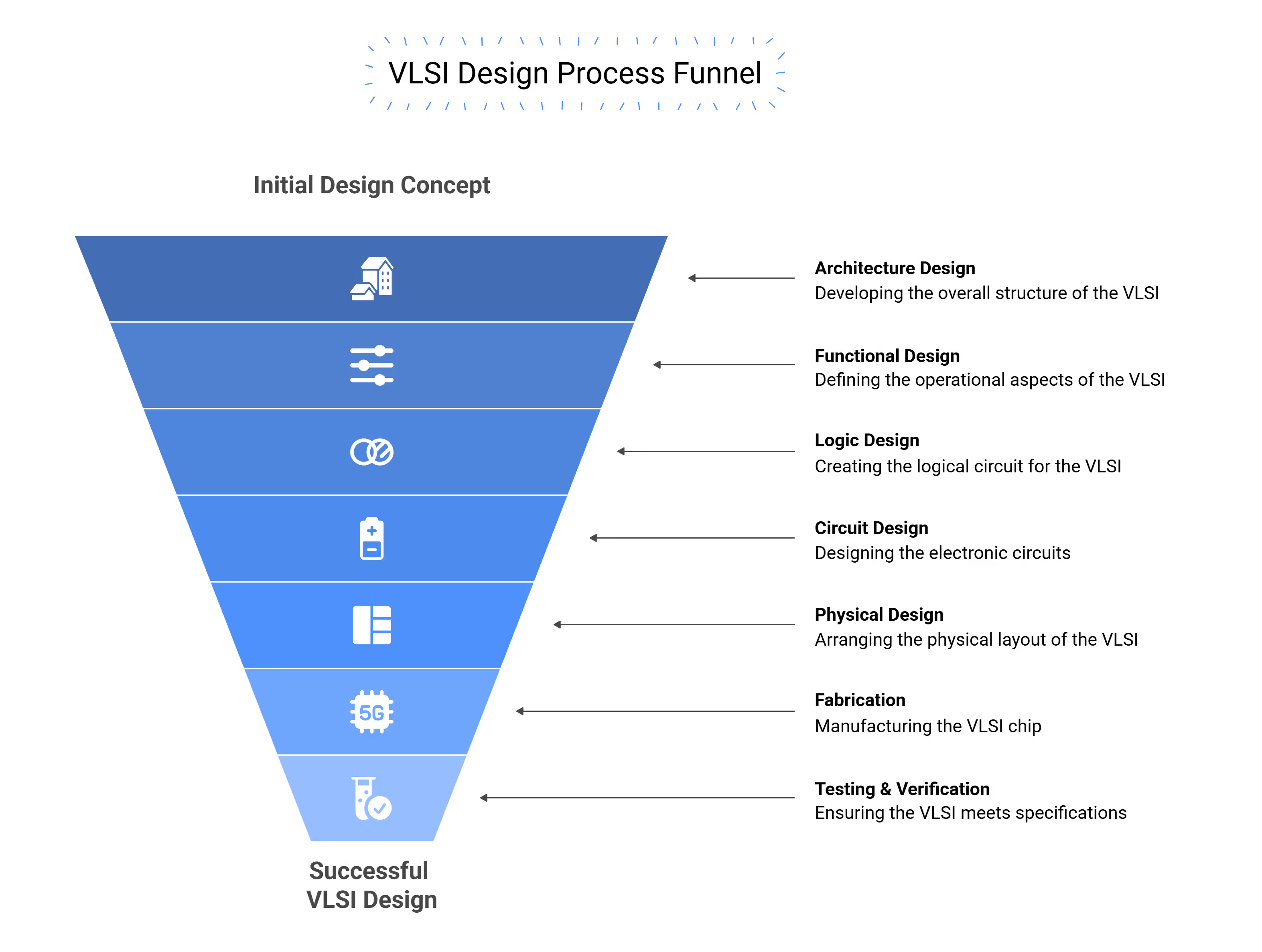
Important Stages in the Design Flow
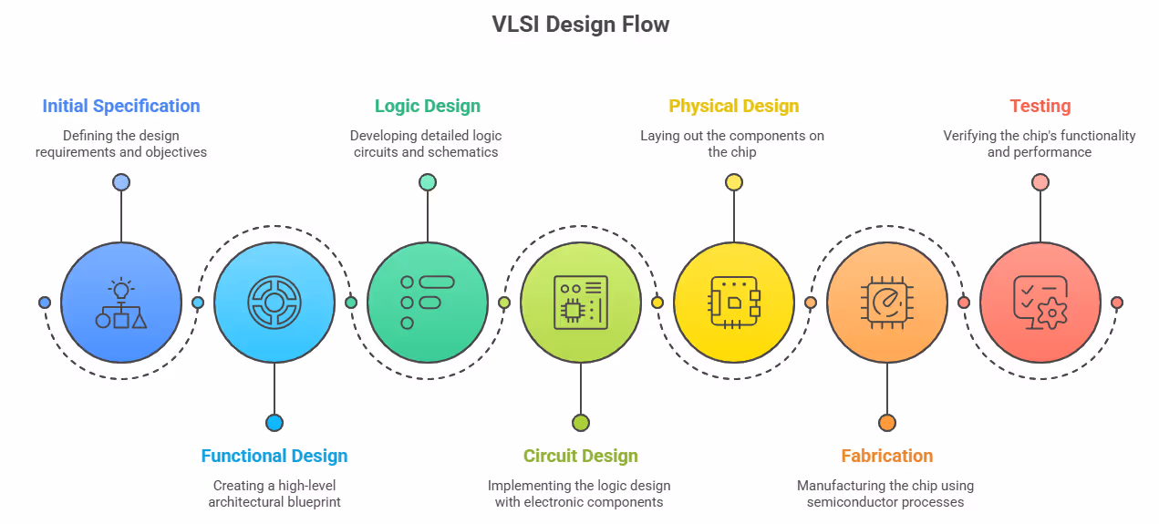
- Specification: Its aim is to define the goals, like functionality, speed, area, and power.
- Architecture Design: This stage describes the system structure. It includes data paths, control logic, and communication between modules.
- Functional Design: The purpose of this stage is to represent each block’s behavior. We use flowcharts or block diagrams here.
- Logic Design: This stage converts functions into Boolean equations and gate-level logic.
- Circuit Design: Here, we develop transistor-level circuits that meet voltage and timing constraints.
- Physical Design: This stage includes the conversion of logical circuits into geometric chip layouts.
- Fabrication: At this level, the layout is manufactured on a silicon wafer.
- Testing & Verification: This is the final stage in this process. Here, we make sure that the chip is working fine and is meeting all the requirements.
What is the Front-End Design Flow in VLSI?
As we have told earlier that the front-end flow deals with the logical behavior of a circuit. It involves both the process of designing as well as verifying. It is carried out before the circuit becomes physical hardware.
Steps in Front-End Design Flow in VLSI
- RTL Design (Register Transfer Level): It involves the writing of design code in Verilog or VHDL.
- Simulation: This step involves checking if the logic behaves correctly under different inputs.
- Functional Verification: It refers to the Validation of the design to see if it meets all requirements.
- Synthesis: Here, the RTL code is converted into a gate-level netlist.
All these steps are important to make sure that all design rules are met before moving to the back-end stage.
What is the Physical Design Flow in VLSI?
The back-end design flow refers to the physical design flow. It focuses on converting the synthesized netlist into an actual physical layout. This final layout can then be fabricated.
Steps in Physical Design Flow in VLSI
- Partitioning: It means dividing the large designs into smaller blocks.
- Floorplanning: At this step, the positions of blocks and macros on the chip are decided.
- Placement: It involves the fixing of standard cell locations for minimal wire length.
- Clock Tree Synthesis (CTS): Here, the balancing of clock delays for all flip-flops is carried out.
- Routing: This stage involves the creation of interconnections between components.
- Physical Verification: At last, it is important to ensure that the layout obeys all design rules, including DRC, LVS, and ERC.
All these steps require powerful EDA (Electronic Design Automation) tools. The commonly used tools are Cadence, Synopsys, and Mentor Graphics.
VLSI Design Flow Diagram
If we want to visually represent how a design will move from an idea to a chip, then we need a VLSI design flow diagram.
This flow will help to check the correctness, efficiency, and manufacturability at every step.
Post-Fabrication Testing and Verification
Once the chip is fabricated, it has to go through an extensive post-silicon validation. Here, the engineers test the real hardware under different environmental as well as electrical conditions to see if:
- The circuit meets functional and timing specifications.
- There are no short circuits or open connections.
- Power and thermal limits are within acceptable ranges.
If the circuit successfully passes all the above tests, the chip moves into mass production.
Tools Used in VLSI Design
We use different tools at each design stage. The purpose is to handle simulation, synthesis, and layout creation. Some popular tools include:
These tools are very helpful for automating the complex design flow. Also, these are important for ensuring precision and performance.
Conclusion
In simple words, the VLSI design flow provides a structured roadmap that helps to convert the concept into the desired silicon. Each step is equally important. From front-end logic creation to back-end physical design and then post-fabrication testing, all are needed to design a chip that is both functional and reliable.
If you are an aspiring chip designer, then you need to properly understand the physical design flow in VLSI. Also, you should know how to interpret the VLSI design flow diagram.
These are the key skills that you need to advance in your career. Upon mastering these concepts, you will open doors to careers in microelectronics, embedded systems, and semiconductor engineering. You can also explore advanced programs like M Tech VLSI for a deeper specialization in this field.
FAQ: VLSI Design Flow
What are the major steps in the VLSI design flow?
Major steps include: specification definition, RTL design, logic synthesis, floorplanning, placement and routing, timing analysis, power and signal integrity checks, verification, fabrication, and testing.
What is RTL design in VLSI?
RTL stands for Register-Transfer Level. It is a design abstraction where hardware functionality is described in terms of data transfers and operations between registers.
What happens during placement and routing in the VLSI flow?
Placement assigns physical positions to logic blocks. Routing connects those blocks with metal layers. The goal is to meet timing, area, and power targets.
How is verification handled in the VLSI design flow?
Verification ensures the design meets specifications by using simulation, formal methods, emulation, and hardware prototyping before fabrication to avoid costly errors.
What is the role of timing and power analysis in VLSI design?
Timing analysis checks that signals meet required timing throughout the chip. Power analysis estimates power consumption and helps in optimizing for low power, especially in portable devices.


M.Tech. in VLSI Design (Executive)
IIT Jammu
Backed by India’s Semiconductor Mission. Built for Long-Term Career Growth.