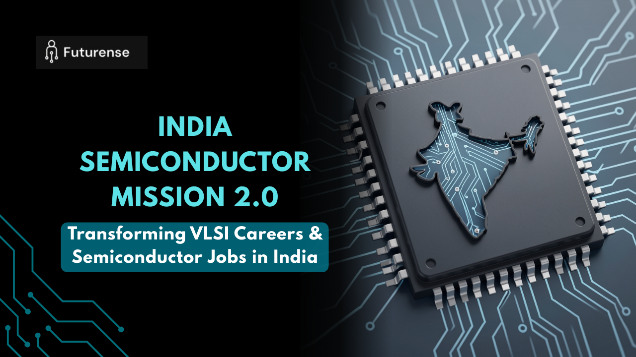


Technology is merely a medium of understanding the advancement of each country. India has been experiencing global growth, and the recent announcement of India Semiconductor Mission 2.0 (ISM) is a game-changer.
The announcement of ISM 2.0 during India’s Union Budget this year has given an open market of ₹40,000 crores outlay. But what is it going to drive and attract? Everything from Supply chain resilience, AI-driven demand, and high-value job creation, to reducing import dependence to a more balanced 30-40%.
What Is India Semiconductor Mission 2.0?
Firstly, the global chip shortages have created a rising demand for the electronics market. This, in turn, has led to a realization of strong domestic semiconductor capabilities of India. In-fact increasing investments in manufacturing, design, and R&D, India is positioning itself as a key player in the global semiconductor jobs ecosystem. This initiative directly impacts VLSI technology, job creation, and long-term innovation.
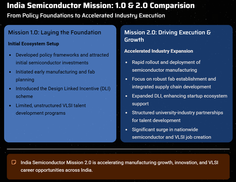
The government has taken the next step that was laid during India Semiconductor Mission 1.0, which mainly focused on creating groundwork, setting policy direction, and attracting global interests of our capabilities. Whereas ISM 2.0 is about making that vision work at scale and execution.
For students and professionals, it opens up new career opportunities across chip design, fabrication, and advanced semiconductor research, making now the right time to explore this growing field. Let us better understand the influence of ISM 1.0 on ISM 2.0.
How India Semiconductor Mission 2.0 Improves Upon ISM 1.0
India’s semiconductor ambitions have evolved significantly with the transition from India Semiconductor Mission (ISM) 1.0 to ISM 2.0. While ISM 1.0 focused on building foundational policies and attracting global interest, ISM 2.0 emphasizes execution, ecosystem expansion, and long-term industry sustainability. The upgraded mission strengthens manufacturing capabilities, expands design incentives, and prioritizes VLSI talent development to support India’s semiconductor growth roadmap.
The comparison below highlights how ISM 2.0 enhances and expands the strategic goals introduced in ISM 1.0.
This progression makes ISM 2.0 more relevant for students, engineers, and professionals looking to build long-term careers in VLSI technology and design based on semiconductor.
At its core, the initiative offers financial incentives to encourage semiconductor fabs, chip assembly units, and display manufacturing facilities to set up operations in India. Alongside manufacturing, there is strong support for chip design through Design-Linked Incentive (DLI) schemes, helping startups and established firms develop and commercialize semiconductor IP locally.
Impact on India’s Semiconductor & VLSI Ecosystem
Understanding the VLSI (Very Large-Scale Integration) ecosystem after the announcement of ISM 2.0 is very important. VLSI is the process of designing and integrating millions to billions of transistors combined in a single semiconductor chip.
The first approach in the industry is make it built in a compact, high-performance, efficient form, which is possible by enabling complex electronic systems. The list of these electronic systems includes processors, memory chips, and system-on-chips (SoCs).
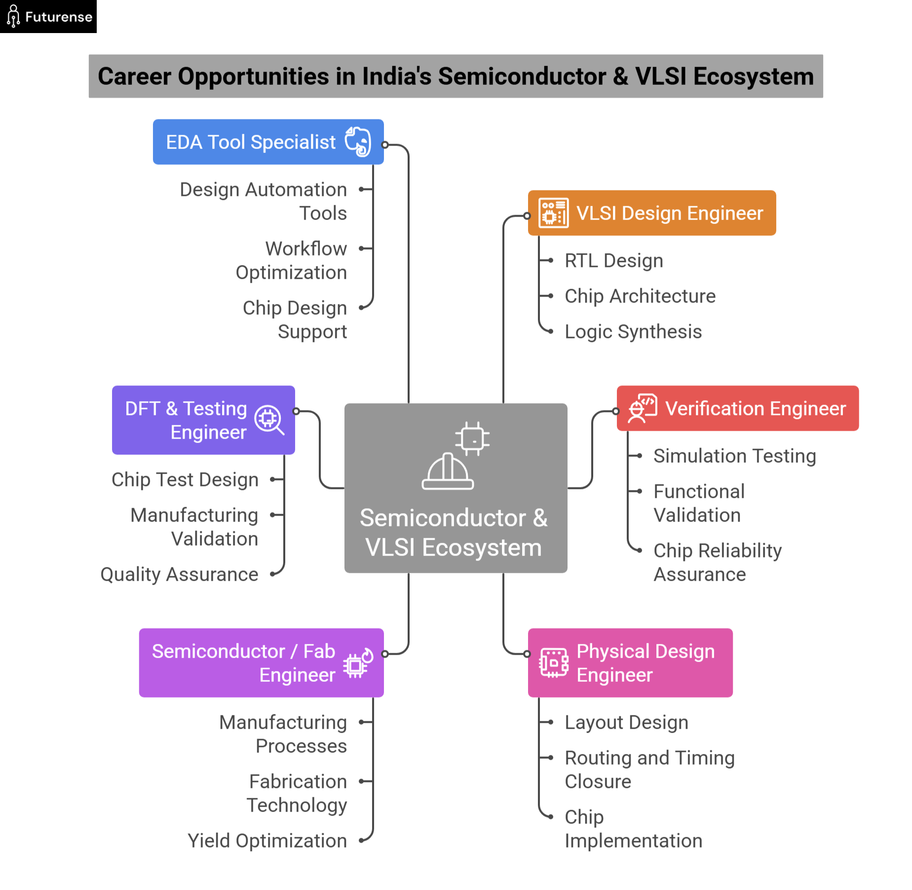
The industries that are getting influenced and impacted by ISM 2.0 are manufacturing, design, and research. Job industries for people who are looking to join as freshers or planning to switch careers are chip architecture, RTL design, verification, physical design, and fabrication.
Core Career Roles in the ISM 2.0 Ecosystem
These roles are directly aligned with the India Semiconductor Mission and VLSI growth:
- VLSI Design Engineer – Works on RTL design, logic synthesis, and chip architecture
- Verification Engineer – Ensures chip functionality using simulation and verification tools
- Physical Design Engineer – Handles layout, placement, routing, and timing closure
- Semiconductor Process / Fab Engineer – Focuses on chip fabrication and manufacturing processes
- DFT & Testing Engineer – Ensures chip reliability and manufacturability
- EDA Tool Specialist – Supports and customizes design automation tools
Career Switching Opportunities Enabled by ISM 2.0
ISM 2.0 also creates clear transition paths for professionals from related fields:
Semiconductor Careers in India: Job Opportunities, Skills, and Education Pathways
ISM 2.0 is creating a strong link between government policies and long-term careers, which in turn urges the requirement of industry expansion. Roles in VLSI design, functional and physical verification, physical design, DFT and testing, process engineering, and semiconductor manufacturing can be options for upskilling for people looking to switch careers.
Equally important is hands-on experience with industry tools and workflows. Employers increasingly prefer candidates who have worked with EDA tools, real-world design problems, and practical projects rather than only theoretical knowledge. This is where industry-aligned training and structured learning paths make a difference.
Advanced certifications and focused VLSI course help bridge the gap between academics and industry expectations by offering practical exposure, mentorship, and project-based learning. With the right mix of fundamentals, hands-on skills, and structured upskilling, students and professionals can confidently prepare for long-term careers in India’s growing semiconductor ecosystem.
TL;DR
India Semiconductor Mission 2.0 is turning policy into real career opportunities by expanding semiconductor manufacturing and VLSI design in India. This growth is creating demand for roles across chip design, verification, physical design, testing, and fabrication.
ECE students, working professionals, and career switchers can all benefit by building strong VLSI fundamentals, gaining hands-on experience with industry tools, and following structured, industry-aligned learning paths. With steady demand, global relevance, and long-term stability, semiconductor and VLSI careers are becoming one of the most reliable options in India’s evolving tech landscape.
FAQs: India Semiconductor Mission 2.0 and VLSI Careers
Which is the top VLSI company in India?
India has several leading VLSI and semiconductor design companies. Some of the top companies include Intel India, Qualcomm, Texas Instruments, AMD, NVIDIA, and Synopsys. Along with global firms, Indian companies like Tata Elxsi, Sasken, and Cyient also play an important role in VLSI design and embedded semiconductor development.
Which Indian Government initiative is supporting VLSI and semiconductor skill development?
The India Semiconductor Mission (ISM) is the primary government initiative supporting semiconductor manufacturing, design, and talent development. It promotes industry-academia collaboration, design-linked incentives (DLI), and investments in semiconductor fabs and research infrastructure.
What is the future of VLSI in India?
The future of VLSI in India is very promising due to increasing demand for chips in AI, automotive, consumer electronics, and telecom industries. With government incentives, global investments, and expanding semiconductor manufacturing, India is expected to become a major hub for chip design and semiconductor innovation, creating strong long-term career opportunities.


M.Tech. in VLSI Design (Executive)
IIT Jammu
Backed by India’s Semiconductor Mission. Built for Long-Term Career Growth.