


Semiconductors are the most used in every electronic device nowadays, like smartphones, laptops, electric vehicles, advanced chips, etc. One of the most popular types of semiconductor technology through doping is called p-type and n-type semiconductors.
Understanding them is necessary for a deeper clarity of electronics, VLSI, and semiconductor engineering. This article discusses what is p and n-type semiconductor, and provides more details.
Why P and N-Type Semiconductors Matter?
Pure silicon or germanium has limited conductivity, hence it is not ideal for most electronic applications. Therefore, engineers add small amounts of impurities to control electrical behavior precisely.
Such a controlled modification helps in the creation of diodes, transistors, Integrated circuits, and microprocessors. Hence, more than academic concepts, they are the p-type and n-type semiconductors.
What Is a Semiconductor?
A semiconductor is a material whose electrical conductivity is between a conductor and an insulator. In its pure form, this is known as an intrinsic semiconductor, and silicon has few free charge carriers at room temperature.
To make it useful, a semiconductor's conductivity should be increased in a controlled manner. Engineers achieve it via doping, leading to the creation of p and n-type semiconductors.
What Is P-Type and N-Type Semiconductor?
What is P-Type Semiconductor?
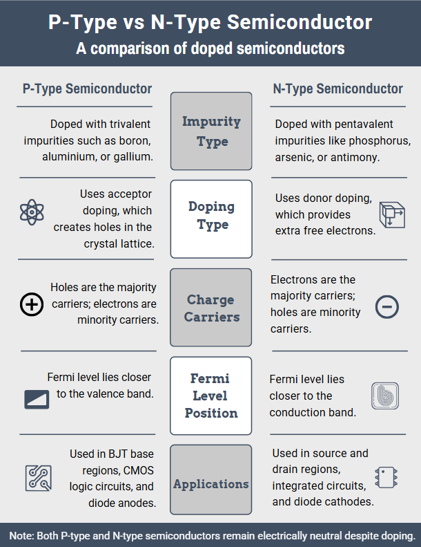
A p-type semiconductor is created by doping a pure semiconductor with trivalent (acceptor) impurities like that as boron, aluminium, or gallium.
Besides p-type semiconductors:
- Impurities have only three valence electrons.
- One bond remains incomplete, thus creating a hole.
- Holes act as positive charge carriers.
Holes act as the majority carriers while electrons are the minority carriers in p-type semiconductors. This is called because holes dominate conduction.
What Is an N-Type Semiconductor?
An n-type semiconductor is created by doping a pure semiconductor with pentavalent (donor) impurities like phosphorus, arsenic, or antimony.
Here, impurity atoms have five valence electrons plus;
- Four electrons form covalent bonds with silicon atoms.
- The fifth electron becomes free and contributes to conduction.
Here, electrons act as majority carriers and holes act as minority carriers. Plus, electrons are negatively charged, hence called n-type.
How Doping Changes Electrical Conductivity?
Doping adds energy levels inside the forbidden energy gap. In an n-type semiconductor, donor atoms provide free electrons easily. Besides, for p-type, acceptor atoms create holes that move through the lattice.
Despite the movement of charge carriers, the overall semiconductor stays electrically neutral as the positive and negative charges in it are balanced.
Moreover, temperature also impacts conductivity. As the temperature increases, carriers get enough energy to participate in conduction.
Energy Band Diagram of N-Type and P-Type Semiconductor
Energy Band Diagram of N-Type Semiconductor
The n-type semiconductor's energy band diagram should be such that:
- Donor energy levels are just below the conduction band.
- Electrons need very little energy to jump into the conduction band.
- The Fermi level shifts closer to the conduction band.
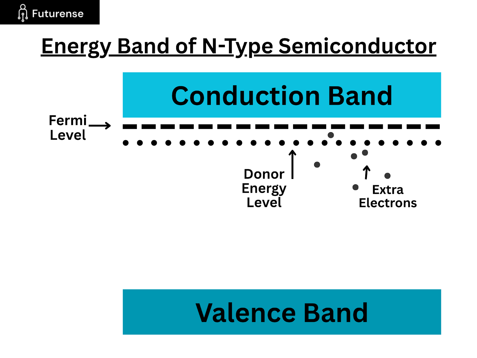
Thus, n-type materials are able to conduct electricity easily.
Energy Band Diagram of P-Type Semiconductor
A p-type semiconductor's energy band diagram should be such that:
- Acceptor energy levels are just above the valence band.
- Electrons move from the valence band to fill holes.
- The Fermi level shifts closer to the valence band.
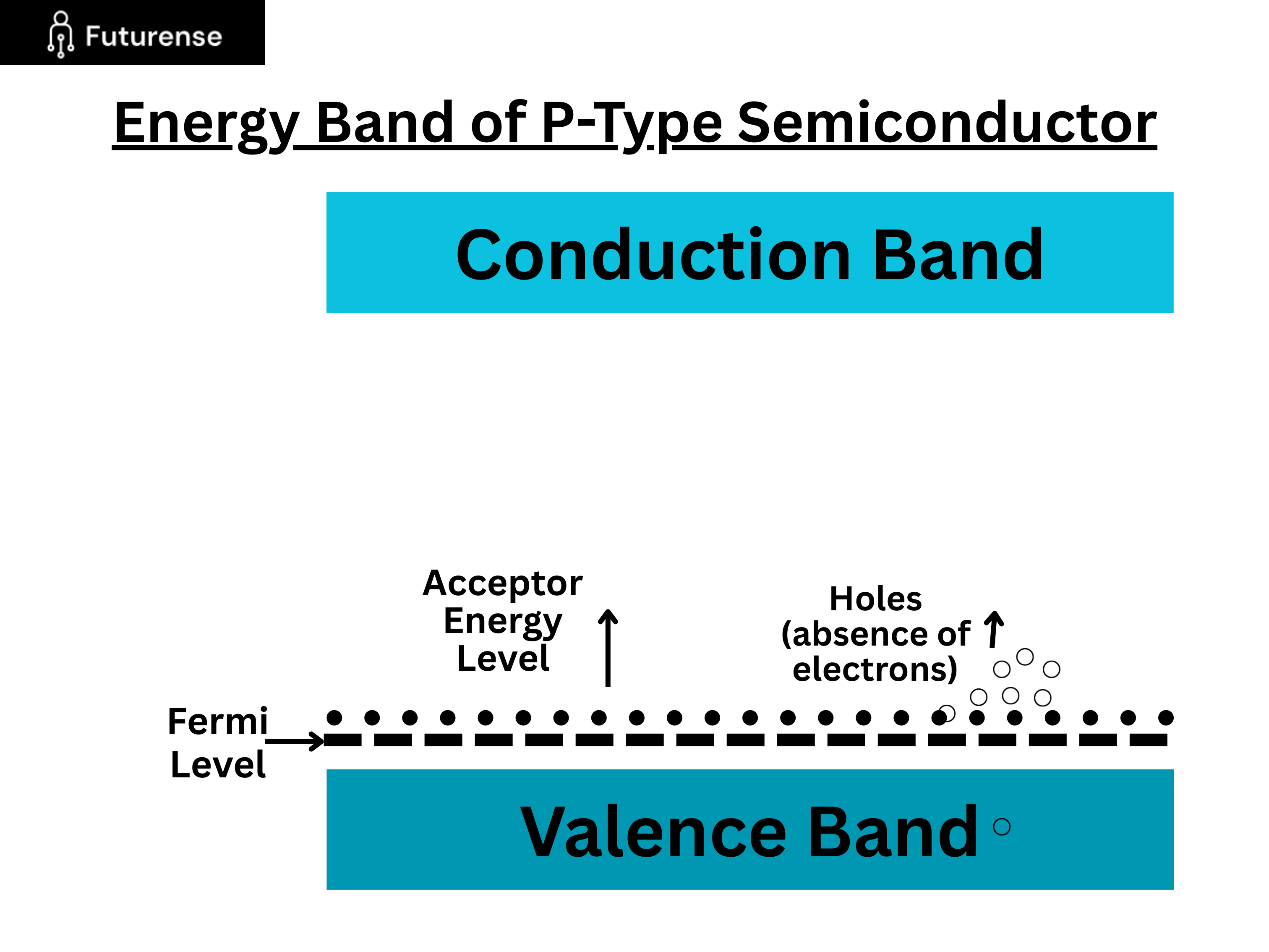
Such a shift justifies hole-dominated conduction.
Why Energy Band Diagrams Matter?
Energy band diagrams are necessary to understand:
- PN junction behavior
- Diodes and transistors
- MOSFET operation
- Integrated circuit design
Hence, without these band diagrams, device physics cannot be understood accurately.
Difference Between P-Type and N-Type Semiconductor
P-Type Semiconductor Examples
Some of the common examples of p-type semiconductors are:
- Silicon doped with boron
- Silicon doped with aluminium
- Germanium doped with gallium
Applications of p-type semiconductors:
- PN junction formation
- Base region of bipolar junction transistors
- CMOS logic circuits
N-Type Semiconductor Examples
Some of the common examples of n-type semiconductors are:
- Silicon doped with phosphorus
- Silicon doped with arsenic
- Germanium doped with antimony
Applications of p-type semiconductors:
- Transistor source and drain regions
- Integrated circuits
- Sensors and detectors
Role of P and N-Type Semiconductors in PN Junctions
- P-type and n-type materials are joined to form a PN junction.
- Electrons and holes diffuse across the junction.
- The depletion region forms with no free carriers.
- An internal electric field develops.
Such a behavior enables the working of diodes, transistors, and Integrated circuits. Besides, every electronic chip has millions to billions of PN junctions.
Real-World Applications of P-Type and N-Type Semiconductors
These have their applications in:
- Microprocessors and memory devices
- Power electronics
- Solar cells
- LEDs and photodiodes
- CMOS technology (combination of nMOS and pMOS)
All of these can't exist without controlled doping, hence the necessity of P and N-type semiconductors.
Why the P and N-Type Semiconductors Concept Is Crucial for VLSI and Semiconductor Careers?
For anyone understanding semiconductor or VLSI careers, p-type and n-type semiconductors are non-negotiable basics. They are important for:
- Device physics
- CMOS fabrication
- Transistor modelling
- Chip verification and design
Hence, advanced semiconductor education is directly gained based upon these concepts.
Common Misconceptions About P-Type and N-Type Semiconductors
Many people have misconceptions about these devices that:
- P-type means positively charged material: This is incorrect, as the material is neutral, so holes are the majority carriers.
- N-type means negative material: It is incorrect, as only holes dominate the conduction.
- Holes are real particles: It is wrong as holes mean the absence of electrons.
Having clarity about these misconceptions is necessary for conceptual understanding.
Final Words
P-type and n-type semiconductors are formed via controlled doping. The aim of regulating electrical conductivity. The type of impurity added determines if these are majority charge carriers, the energy band structure, and the electrical behavior.
They are crucial to understand, as these are fundamental to modern electronics, from simple diodes to advanced microprocessors. Hence, having proficiency in its understanding is necessary to understand the digital world's technicalities.
FAQ : P-Type and N-Type Semiconductor
What is the difference between P and N junctions?
A P junction has holes as majority carriers, while an N junction has electrons as majority carriers. When joined, they form a PN junction used in diodes and transistors.
What are examples of pentavalent and trivalent impurities?
Pentavalent impurities include phosphorus, arsenic, and antimony. Trivalent impurities include boron, aluminium, and gallium.
Why is it called p-type?
It is called p-type because holes (positive charge carriers) dominate electrical conduction in the material.
What is the difference between p and n?
The key difference lies in charge carriers: p-type semiconductors conduct mainly through holes, while n-type semiconductors conduct mainly through electrons.
Is n-type semiconductor positive or negative?
An n-type semiconductor is electrically neutral. Although electrons are majority carriers, the material itself has no net charge.
Why is it called n-type?
It is called n-type because electrons (negative charge carriers) are the majority carriers responsible for conduction.


M.Tech. in VLSI Design (Executive)
IIT Jammu
Backed by India’s Semiconductor Mission. Built for Long-Term Career Growth.


.avif)