
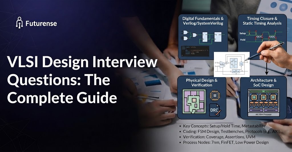


VLSI design interview questions typically span four areas: digital electronics fundamentals, RTL design and coding, verification methodology, and physical design or STA, depending on the role you're interviewing for. This guide covers 50+ real interview questions across all four areas, with answers written the way you'd actually explain them in an interview room, not textbook definitions.
VLSI, or Very Large Scale Integration, is the process of designing integrated circuits by packing millions of transistors onto a single chip, and interview panels test this concept from multiple angles: theory, tool usage, and problem-solving under pressure. Before you dive into specific questions, it helps to understand what VLSI design and its applications actually cover, since interviewers often open with a scope question to gauge how well you understand the field before drilling into specifics.
Interview difficulty and question mix depend heavily on the role. A fresher interviewing for an RTL design position gets a different question set than a candidate interviewing for a physical design or DFT role. This guide is organized by the actual sections companies test, in the order most panels use them.
Basic VLSI Design Interview Questions for Freshers
These are the questions that show up in almost every VLSI interview, regardless of specialization. Panels use them to check whether your fundamentals are solid before moving to role-specific depth.
What is VLSI and why is it important?
VLSI stands for Very Large Scale Integration, the technology of combining millions or billions of transistors onto a single silicon chip. It matters because it's what makes modern processors, memory chips, and mobile SoCs possible; without VLSI, we'd still be building circuits from individual discrete components.
What is the Difference Between Analog and Digital VLSI Design?
Analog VLSI design deals with continuous signal circuits, amplifiers, ADCs, DACs, power management ICs, where signal fidelity and noise margins matter most. Digital VLSI design deals with discrete logic states (0s and 1s) and focuses on timing closure, area, and power optimization. Most VLSI job openings in India are digital design roles, so expect more depth-testing there.
What is the Difference Between Combinational and Sequential Circuits?
Combinational circuits produce outputs that depend only on current inputs, with no memory of past states, such as adders and multiplexers. Sequential circuits, like flip-flops and counters, have outputs that depend on both current inputs and previous states, because they store state using clock-triggered elements. This distinction between combinational and sequential circuits comes up constantly in both design and verification interviews, so be ready to give circuit examples on the spot.
What is the Difference Between Latch and Flip-Flop?
A latch is level-sensitive, meaning it's transparent and passes data through as long as the enable signal is active. A flip-flop is edge-sensitive, capturing data only at the clock edge (rising or falling). Flip-flops are preferred in synchronous digital design because they avoid the timing hazards latches can introduce in a clocked system.
What is Setup Time and Hold Time?
Setup time is the minimum time before the clock edge that data must be stable at a flip-flop's input. Hold time is the minimum time after the clock edge that data must remain stable. Violating either causes metastability, an unpredictable output state, which is why timing closure is such a heavily tested topic in VLSI interviews.
What are P-Type and N-Type Semiconductors?
A P-type semiconductor has an excess of holes (positive charge carriers) created by doping with trivalent elements like boron. An N-type semiconductor has an excess of electrons created by doping with pentavalent elements like phosphorus. Understanding p-type and n-type semiconductors is foundational because CMOS logic, the basis of nearly all modern digital chips, is built entirely from PMOS and NMOS transistor pairs.
RTL Design and Coding Interview Questions
Once fundamentals are confirmed, interviewers move into RTL (Register Transfer Level) design questions, testing whether you can actually write synthesizable Verilog or VHDL, not just describe concepts.
What is the Difference Between Blocking and Non-Blocking Assignments in Verilog?
Blocking assignments (=) execute sequentially within a procedural block, each statement finishes before the next begins. Non-blocking assignments (<=) schedule updates to happen at the end of the current simulation time step, allowing parallel-like behavior. The standard rule interviewers expect: use blocking for combinational logic and non-blocking for sequential (clocked) logic.
Write Verilog Code for a D Flip-Flop with Asynchronous Reset.
A working answer describes an always block sensitive to the positive clock edge and the reset signal, where the reset condition is checked first and takes priority regardless of the clock. Interviewers are checking two things here: correct sensitivity list syntax, and whether you understand that asynchronous reset must appear in the sensitivity list itself, not just inside the block body.
What is the Difference Between a Multiplexer and a Demultiplexer?
A multiplexer selects one of several input signals and routes it to a single output, based on select lines. A demultiplexer does the reverse, taking one input and routing it to one of several outputs. Both are building blocks tested in RTL coding rounds, often as a live coding exercise rather than a verbal question.
What is a Race Condition in RTL Design and How do you Avoid it?
A race condition occurs when the output of a circuit depends on the relative timing of two or more signals, and different orderings can produce different results. In RTL, this typically arises from mixing blocking and non-blocking assignments incorrectly, or from multiple always blocks writing to the same signal. Avoiding it comes down to disciplined coding style: non-blocking assignments for all sequential logic, and never assigning the same signal from two different always blocks.
What is the Significance of Parameterized Modules in Verilog?
Parameterized modules let you write reusable RTL code where widths, depths, or other constants are configurable at instantiation time rather than hardcoded. This matters in real design work because the same adder or FIFO module can be reused across a 8-bit and a 32-bit datapath without duplicating code, which is exactly the kind of scalable thinking interviewers want to see from a design engineer.
VLSI Verification Interview Questions
Verification is one of the highest-paying and most in-demand VLSI specializations, so verification-specific interviews go deep on methodology, not just RTL basics.
What is the Difference Between Verification and Validation in VLSI?
Verification confirms that the design meets its specification, "did we build the design right", typically done through simulation before tapeout. Validation confirms that the design meets the actual system requirements in the real world, "did we build the right design", often tested on silicon after fabrication. Confusing the two is a common fresher mistake that interviewers specifically probe for.
What is UVM and Why is it used?
UVM (Universal Verification Methodology) is a standardized, class-based verification framework built on SystemVerilog that provides reusable components, drivers, monitors, scoreboards, sequences, for building testbenches. It's used because it standardizes verification environments across projects and companies, so verification engineers can move between teams without relearning the entire testbench architecture from scratch.
What is the Difference Between Directed Testing and Constrained Random Verification?
Directed testing writes specific test cases targeting specific scenarios, predictable but limited in coverage. Constrained random verification generates randomized stimulus within defined constraints, exploring corner cases a human might never think to write manually. Most modern verification environments combine both: directed tests for known critical paths, constrained random for coverage closure.
What is Functional Coverage and Why Does it Matter?
Functional coverage tracks which functional scenarios and corner cases have actually been exercised during simulation, distinct from code coverage, which only tracks which lines of code executed. A design can have 100% code coverage and still miss critical functional scenarios, which is why verification sign-off depends on functional coverage closure, not just code coverage numbers.
What is a Scoreboard in UVM and What Does it do?
A scoreboard is a UVM component that checks whether the actual output (DUT response) matches the expected output, usually generated by a reference model. It's the component that actually determines pass or fail for a test, everything else in the testbench (drivers, monitors, sequences) exists to feed data into and out of the scoreboard correctly.
What is the Difference Between Assertion-Based Verification and Simulation-Based verification?
Assertion-based verification uses formal properties (typically written in SystemVerilog Assertions) to check design behavior continuously during simulation or through formal proof, catching bugs closer to their source.
Simulation-based verification relies on running testbenches and checking outputs after the fact. Most real verification environments use both together, assertions for local, protocol-level checks, and simulation-based scoreboards for end-to-end functional correctness.
Physical Design and STA Interview Questions
Physical design interviews test whether you understand what happens after RTL is synthesized, floorplanning, placement, routing, and timing closure, which is where a design actually becomes manufacturable silicon.
What is Floorplanning in VLSI Physical Design?
Floorplanning is the stage where the chip's major blocks, macros, and I/O pads are arranged on the die area before detailed placement and routing begin. Good floorplanning decisions early on directly affect timing closure and routing congestion later, which is why senior physical design engineers spend disproportionate time getting this stage right.
What is Static Timing Analysis (STA) and Why is it used Instead of Simulation for Timing Checks?
Static timing analysis checks every timing path in a design against setup and hold constraints without needing to simulate actual input vectors, making it exhaustive across all possible paths. Simulation only checks timing for the specific vectors you run, so it can miss rare paths entirely. STA is preferred for timing sign-off because it's both faster and mathematically exhaustive.
What is Clock Skew and Why Does it Matter?
Clock skew is the difference in arrival time of a clock signal at different flip-flops in a design, caused by differences in wire length or buffering along the clock tree. Excessive skew can cause setup or hold violations even in a logically correct design, which is why clock tree synthesis (CTS) is treated as its own dedicated stage in the physical design flow.
What is the Difference Between Placement and Routing?
Placement determines the physical (x, y) location of each standard cell on the die. Routing then creates the actual metal wire connections between those placed cells according to the netlist. Placement quality directly constrains how well routing can succeed, a poor placement can make a design unroutable or force excessive detours that hurt timing.
What Causes Hold Violations and How are they Typically Fixed?
Hold violations occur when data changes too quickly relative to the clock, arriving at the next flip-flop before the required hold time has elapsed, usually on very short paths. They're typically fixed by inserting delay buffers on the offending path to slow down data arrival just enough to satisfy the hold requirement, without affecting the setup timing on that same path.
How VLSI Interview Difficulty Changes by Experience Level
Interview panels calibrate difficulty and depth based on your stated experience level, and knowing what's expected at each stage helps you prepare the right depth instead of over- or under-preparing.
If you're prepping at the fresher or early-career stage, spend most of your time on the fundamentals and RTL sections above. If you're interviewing at a senior level, panels expect you to speak in terms of trade-offs and real project decisions, not textbook answers.
How to Prepare for a VLSI Interview: A Practical Checklist
Knowing the questions is only half the preparation. Here's what actually moves the needle in the interview room.
- Re-derive, don't memorize: Interviewers can tell within two follow-up questions whether you memorized an answer or actually understand the concept. Be able to explain setup/hold time or STA from first principles, not just recite the definition.
- Practice writing RTL by hand: Many companies still ask you to write Verilog on a whiteboard or shared doc without an IDE. Practice basic modules (flip-flops, FSMs, simple arithmetic blocks) without autocomplete.
- Know your own project deeply: Whatever project or tapeout you list on your resume will get drilled into far beyond what the question bank above covers. Be ready to explain design decisions you made and trade-offs you weighed.
- Brush up on the specific sub-domain of the role: A verification interview and a physical design interview overlap on fundamentals but diverge sharply after that. Tailor your prep to the actual job description, not a generic VLSI question list.
If your fundamentals in digital design or your hands-on tool exposure feel thin heading into interviews, a structured program like IIT Jammu's M.Tech in VLSI Design is built specifically to close that gap with hands-on RTL, verification, and physical design coursework rather than just theory.
Once you've cleared the interview, it's worth knowing what comes next. Read up on VLSI career paths in India for the bigger role-progression picture, or check current VLSI engineer salary in India data if you're currently evaluating an offer.
TL;DR
This guide covers 50+ VLSI design interview questions with interview-ready answers across four key areas: digital electronics fundamentals, RTL design & Verilog coding, VLSI verification (UVM), and physical design/STA. It explains what interviewers expect at the fresher, mid-level, and experienced stages, highlights frequently asked concepts like setup/hold time, blocking vs. non-blocking assignments, UVM, functional coverage, floorplanning, and static timing analysis, and ends with practical preparation tips such as mastering fundamentals, practicing RTL coding, and understanding your projects thoroughly.
What are the most commonly asked VLSI interview questions?
The most commonly asked VLSI interview questions cover digital electronics fundamentals (combinational vs. sequential circuits, setup/hold time), basic RTL coding (blocking vs. non-blocking assignments), and an overview of the VLSI design flow from RTL to tapeout. These come up regardless of which specific VLSI role you're interviewing for.
How do I prepare for a VLSI interview as a fresher?
Freshers should focus on digital electronics fundamentals, basic Verilog or VHDL coding, and being able to explain the overall VLSI design flow clearly. Practice writing simple RTL modules by hand, and be ready to explain any academic project involving digital design or FPGA work in detail.
What is asked in a VLSI physical design interview?
VLSI physical design interviews typically cover floorplanning, placement and routing concepts, static timing analysis (STA), clock tree synthesis, and how to debug setup or hold violations. Experienced candidates should also expect questions about trade-offs between area, power, and timing closure.
What is asked in a VLSI verification interview?
VLSI verification interviews focus heavily on UVM methodology, the difference between directed and constrained random testing, functional coverage versus code coverage, and how scoreboards and assertions work together in a testbench. Expect scenario-based debugging questions at the mid-to-senior level.


M.Tech. in VLSI Design (Executive)
IIT Jammu
Backed by India’s Semiconductor Mission. Built for Long-Term Career Growth.